 |
|
| |
|
|
业务洽谈:
联系人:张顺平
手机:17727550196(微信同号)
QQ:3003262363
EMAIL:zsp2018@szczkjgs.com
联系人:鄢先辉
手机:17727552449 (微信同号)
QQ:2850985542
EMAIL:yanxianhui@szczkjgs.com
负责人联络方式:
手机:13713728695(微信同号)
QQ:3003207580
EMAIL:panbo@szczkjgs.com
联系人:潘波 |
|
|
| |
|
 |
|
 |
当前位置:首页 -> 方案设计 |
|
|
| bq25120可穿戴和IoT电池充电器解决方案 |
|
|
| 文章来源: 更新时间:2015/11/11 15:48:00 |
|
TI公司的bq25120是高度集成电池充电管理集成电路,包括用于可穿戴设备的线性充电器,稳压输出,负载开关,带定时器的人工重置以及电池电压监视器,工作电压高达4.65 V,主要用在智能手表和其它可穿戴设备,健身设备附件,健康监测附件以及可充电玩具.本文介绍了bq25120主要特性,框图和应用电路,以及评估板bq25120EVM-731主要特性,电路图,材料清单和PCB设计文件图.
The bq25120 is a highly integrated battery charge management IC that integrates the most common functions for wearable devices: Linear charger, regulated output, load switch, manual reset with timer, and battery voltage monitor. The integrated buck converter is a high efficiency, low IQ switcher using DCS control that extends light load efficiency down to 10-µA load currents.The low quiescent current during operation and shutdown enables maximum battery life. The device supports charge currents from 5 mA to 300 mA. The input current limit, charge current, buck converter output voltage, LDO output voltage, and other parameters are programmable through the I2C interface.
The battery is charged using a standard Li-Ion charge profile with three phases: precharge, constant current and constant voltage. A voltage-based JEITA compatible battery pack thermistor monitoring input (TS) is included that monitors battery temperature and automatically changes charge parameters to prevent the battery from charging outside of its safe temperature range. The charger is optimized for 5-V USB input, with 20-V tolerance to withstand line transients. The buck converter is run from the input or battery. When in battery only mode, the device can run from a battery up to 4.65 V.
A configurable load switch allows system optimization by disconnecting infrequently used devices. The manual reset with timer allows mutliple different configuration options for wake are reset optimization. A simple voltage based monitor provides battery level information to the host in 2% increments from 60% to 100% of the programmed V(BATREG).
bq25120主要特性:
Increases System Operation Time Between Charges
Configurable 300-mA Buck Regulator (1.8-V Default)
700 nA (typical) Iq with Buck Converter Enabled (No Load)
Configurable Load Switch or 100mA LDO Output (Load Switch by Default)
Up to 300-mA Charge Current for Fast Charging
0.5% Accurate Battery Voltage Regulation (Configurable from 3.6 V to 4.65 V in 10-mV Steps)
Configurable Termination Current Down to 500 µA
Simple Voltage Based Battery Monitor
Highly Integrated Solution with Small Footprint
2.5 mm × 2.5 mm WCSP Package and 6 External Components for Minimal Solution
Push-Button Wake-Up and Reset with Adjustable Timers
Power Path Management for Powering the
System and Charging the Battery
Power Path Management enables <50 nA Ship Mode Battery Quiescent Current for Longest Shelf Life
Battery Charger Operates from 3.4 V – 5.5 VIN (5.5-V OVP / 20-V Tolerant)
Dedicated Pins for Input Current Limit, Charge Current, Termination Current, and Status Output
I2C Communication Control
Charge Voltage and Current
Termination Threshold
Input Current Limit
VINDPM Threshold
Timer Options
Load Switch Control
Controls for Interrupts for Faults and Status
System Output Voltage Adjustment
LDO Output Voltage Adjustment
bq25120应用:
Smart Watches and other Wearable Devices
Fitness Accessories
Health Monitoring Medical Accessories
Rechargeable Toys
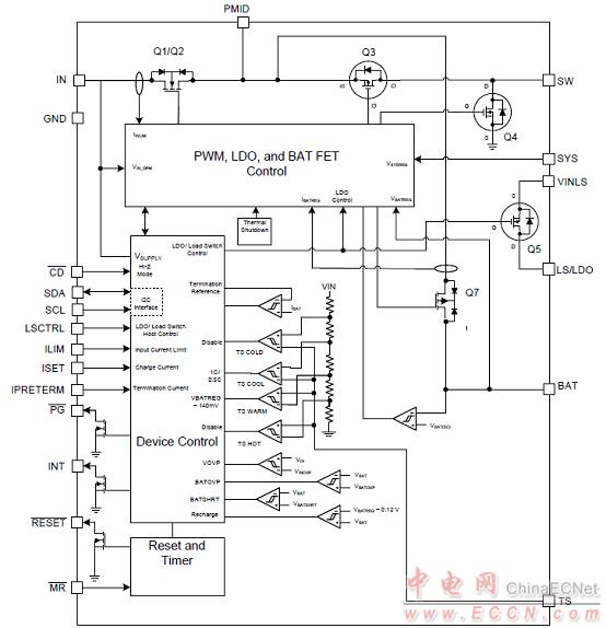
图1.bq25120功能框图

图2.bq25120应用电路图
评估板bq25120EVM-731
The bq25120EVM-731 evaluation module is a highly integrated battery charge management IC that integrates the most common functions for wearables devices: Linear charger, regulated output, load switch, manual reset with timer, and battery voltage monitor. The low quiescent current during operation and shutdown enables amaximum battery life. The device supports charge currents from 5 mA to 300 mA. The input current limit, charge current, PWM output voltage, LDO output voltage, and other parameters are programmable through the I2C interface. The battery is charged using a standard Li-Ion charge profile with three phases: precharge, constant current and constant voltage.
The bq25120 EVM on PWR731 PCB is a complete battery power management module for evaluatingcompact, highly-integrated, flexible, high efficiency, linear charging solution for single cell, Li-Ion and Li-Polymer battery-powered systems used in wearables and low-power portable applications.
评估板bq25120EVM-731主要特性:
• Configurable 300-mA buck regulator (1.8-V default)
• 700-nA typical IQ with PWM enabled
• 0.5% accurate battery voltage regulation (configurable from 3.6 V to 4.65 V in 10-mV steps)
• Configurable termination current down to 500 μA
• 2.5 mm × 2.5 mm WCSP package and 6 external components for minimum solution
• Power path management for powering the system and charging the battery
• Power path management enables < 150 nA ship mode battery quiescent current for longest shelf life
• Push-button wake-up and reset with adjustable timers
• Battery charger operates from 3.4 V – 5.5 V VIN (5.5-V OVP / 20-V tolerant)
• I2C control of key parameters
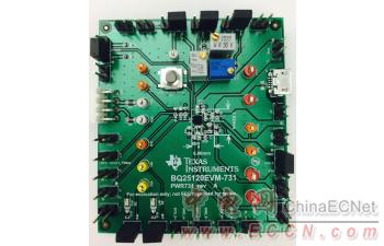
图3.评估板bq25120EVM-731外形图
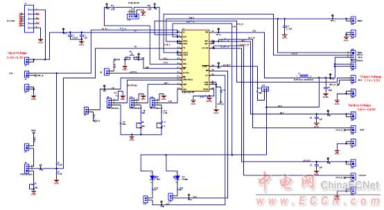
图4.评估板bq25120EVM-731电路图
评估板bq25120EVM-731材料清单:
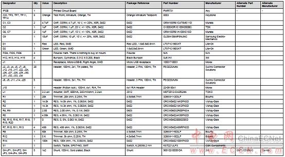
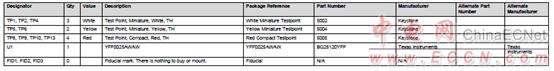
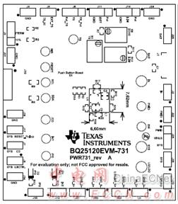
图5.评估板bq25120EVM-731 PCB设计图(1)

图6.评估板bq25120EVM-731 PCB设计图(2)
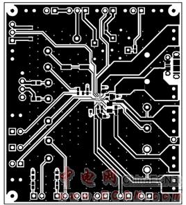
图7.评估板bq25120EVM-731 PCB设计图(3)
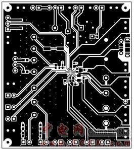
图8.评估板bq25120EVM-731 PCB设计图(4)
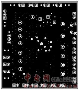
图9.评估板bq25120EVM-731 PCB设计图(5)
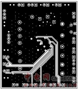
图10.评估板bq25120EVM-731 PCB设计图(6)
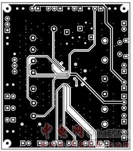
图11.评估板bq25120EVM-731 PCB设计图(7)
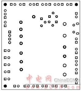
图12.评估板bq25120EVM-731 PCB设计图(8)
|
|
| |
| |
|
|
|