 |
|
| |
|
|
ҵ��Ǣ̸��
��ϵ�ˣ���˳ƽ
�ֻ���17727550196����ͬ�ţ�
QQ:3003262363
EMAIL:zsp2018@szczkjgs.com
��ϵ�ˣ�۳�Ȼ�
�ֻ���17727552449 ����ͬ�ţ�
QQ:2850985542
EMAIL:yanxianhui@szczkjgs.com
���������緽ʽ��
�ֻ���13713728695����ͬ�ţ�
QQ:3003207580
EMAIL:panbo@szczkjgs.com
��ϵ�ˣ��˲� |
|
|
| |
|
 |
|
 |
��ǰλ�ã���ҳ -> �������� |
|
|
| TLE9879 BLDC������������ |
|
|
| ������Դ���������Ƽ� ����ʱ�䣺2019/11/30 9:51:00 |
|
infineon��˾��TLE9879QXA40�ǵ�Ƭ��������������,�����˹�ҵ����ARM® Cortex® M3��,����ʵ���Ƚ�����������㷨��ų��������(FOC).TLE9879��������ȫ���ɵ�NFET������,ͨ����ӹ���NFET��������������,��ɱÿ��Ե͵�ѹ����,�ɱ�̵����͵���б�ʿ��ƾ��������EMC����.���������������������,��������PWM���ƵIJ���ͱȽϵ�ͬ����αƽ�ADC��16λ��ʱ��.�������LIN�շ���ʹ���ܺ�ͨ��I/O���豸����ͨ��.��������Ƭ�����Ե�ѹ��ѹ�����ⲿ���ع���.�߶ȼ��ɵ�����������ģ������ֹ�������,Ƕ���32λ������(����Ƶ�ʸߴ�40MHz)����ϵͳ�ͽӿڿ���.Ƭ�ϵ�ѹ������ѹ���������ڲ����ⲿ����.�ڲ������ṩ�ɱ�Ч���ʱ��,�ر��ʺ���LINͨ��.��LIN�շ�������ͨ�Žӿ�.�������˾������MOSFET�������Ż�BLDC�����ŵ�������,����PWM����,�������Ժ͵�ɱ�����,��10λSAR ADCʵ�ָ߾��ȴ���������,��8λADC������ϲ���.����Դ5.5 V- 27 V����,�����¶�Tj = -40�浽+150��,����AEC ��֤,��Ҫ������������������úͷ���.���Ľ�����TLE9879QXA40��Ҫ����,��ͼ,ϵͳ���Ƶ�Ԫ-����ģ���ͼ��Cortex-M3��ͼ,������TLE9879 EvalKit V1.3��Ҫ����,��ͼ,��·ͼ,Ԫ������ͼ��PCB���ͼ.
The TLE9879QXA40 is a single chip 3-Phase motor driver that integrates the industry standard ARM® Cortex® M3core, enabling the implementation of advanced motor control algorithms such as field-oriented control.
It includes six fully integrated NFET drivers optimized to drive a 3-Phase motor via six external power NFETs, acharge pump enabling low voltage operation and programmable current along with current slope control foroptimized EMC behavior. Its peripheral set includes a current sensor, a successive approximation ADCsynchronized with the capture and compare unit for PWM control and 16-bit timers. A LIN transceiver is also integrated to enable communication to the device along with a number of general purpose I/Os. It includes anon-chip linear voltage regulator to supply external loads.It is a highly integrated automotive qualified device enabling cost and space efficient solutions for mechatronicBLDC motor drive applications such as pumps and fans.
This highly integrated circuit contains analog and digital functional blocks. An embedded 32-bit microcontroller isavailable for system and interface control. On-chip, low-dropout regulators are provided for internal and externalpower supply. An internal oscillator provides a cost effective clock that is particularly well suited for LINcommunications. A LIN transceiver is available as a communication interface. Driver stages for a Motor Bridge orBLDC Motor Bridge with external MOSFET are integrated, featuring PWM capability, protection features and acharge pump for operation at low supply voltage. A 10-bit SAR ADC is implemented for high precision sensormeasurement. An 8-bit ADC is used for diagnostic measurements.
The Micro Controller Unit supervision and system protection (including a reset feature) is complemented by aprogrammable window watchdog. A cyclic wake-up circuit, supply voltage supervision and integrated temperaturesensors are available on-chip.
All relevant modules offer power saving modes in order to support automotive applications connected to terminal30. A wake-up from power-save mode is possible via a LIN bus message, via the monitoring input or using aprogrammable time period (cyclic wake-up).
Featuring LTI, the integrated circuit is available in a VQFN-48-31 package with 0.5 mm pitch, and is designed towithstand the severe conditions of automotive applications.
The TLE9879QXA40 has several operation modes mainly to support low power consumption requirements.
TLE9879QXA40��Ҫ����:
• 32 bit ARM Cortex M3 Core
�C up to 40 MHz clock frequency
�C one clock per machine cycle architecture
• On-chip memory
�C 128 kByteFlash including
�C 4 kByte EEPROM (emulated in Flash)
�C 512 Byte 100 Time Programmable Memory (100TP)
�C 6 kByte RAM
�C Boot ROM for startup firmware and Flash routines
• On-chip OSC and PLL for clock generation
�C PLL loss-of-lock detection
• MOSFET driver including charge pump
• 10 general-purpose I/O Ports (GPIO)
• 5 analog inputs, 10-bit A/D Converter (ADC1)
• 16-bit timers - GPT12, Timer 2, Timer 21 and Timer 3
• Capture/compare unit for PWM signal generation (CCU6)
• 2 full duplex serial interfaces (UART) with LIN support (for UART1 only)
• 2 synchronous serial channels (SSC)
• On-chip debug support via 2-wire SWD
• 1 LIN 2.2 transceiver
• 1 high voltage monitoring input
• Single power supply from 5.5 V to 27 V
• Extended power supply voltage range from 3 V to 28 V
• Low-dropout voltage regulators (LDO)
• High speed operational amplifier for motor current sensing via shunt
• 5 V voltage supply for external loads (e.g. Hall sensor)
• Core logic supply at 1.5 V
• Programmable window watchdog (WDT1) with independent on-chip clock source
• Power saving modes
�C MCU slow-down Mode
�C Sleep Mode
�C Stop Mode
�C Cyclic wake-up Sleep Mode
• Power-on and undervoltage/brownout reset generator
• Overtemperature protection
• Short circuit protection
• Loss of clock detection with fail safe mode entry for low system power consumption
• Temperature Range Tj = -40�� to +150��
• Package VQFN-48 with LTI feature
• Green package (RoHS compliant)
• AEC qualified
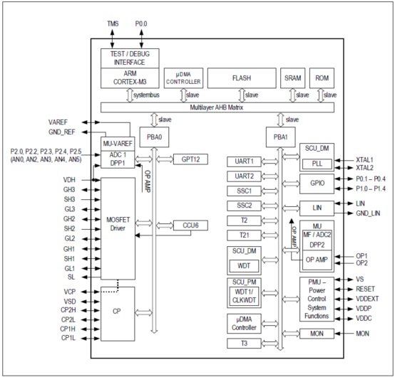
ͼ1.TLE9879QXA40��ͼ
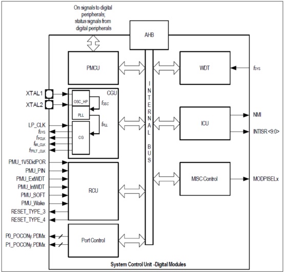
ͼ2.ϵͳ���Ƶ�Ԫ-����ģ���ͼ
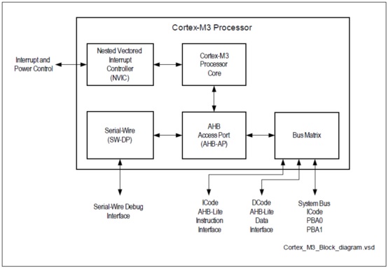
ͼ3. Cortex-M3��ͼ
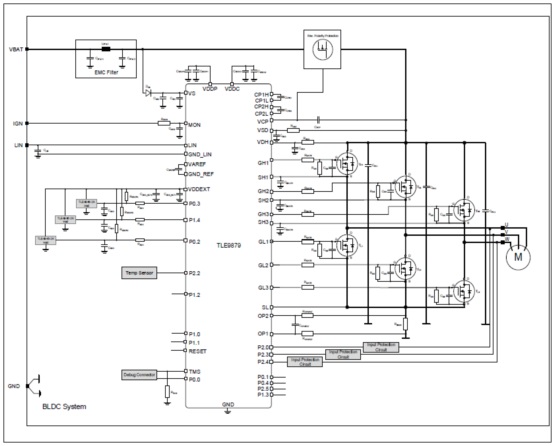
ͼ4.TLE9879QXA40��Ӧ�ÿ�ͼ
Ӧ�ÿ�ͼ���Ԫ����:
������TLE9879 EvalKit V1.3
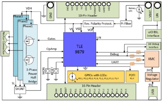
This board provides a simple, easy-to-use tool for getting familiar with Infineon��s Embedded Power ICTLE9879QXA40 (further to be named: TLE9879). It contains the TLE9879 and its typical application circuitincluding three MOSFET half bridges to drive a BLDC motor. The board is ready to connect with car supply orsimilar and has an onboard J-Link debugger.
All relevant chip pins are connected to pin headers at the edge of the board, where signals can be probed orapplied directly (see Table 2, Table 3). By different jumper settings LEDs can be put in parallel to several portsand selected functions can be configured (see Table 6). Push button switches allow easy hardware reset and triggering of the MON input. There are intended test points for all six gate driver pins, for measurements at theshunt, VDDC and several ground points on the evaluation board (see Figure 3). For testing analog signals ADCinputs can be varied by the potentiometer on board. Three phases of motor current can be picked off at a terminal block to connect a DC brushless motor.
The evaluation board can be operated by standard laboratory equipment as power supply and LINcommunication are working via banana jacks. Debugging and UART are provided via an USB interface combinedwith an onboard Segger J-Link (XMC4200). Bidirectional level shifters ensure that the respective XMC pins are in tristate as long as UART or debugging is not used.
An SWD interface is available to use another ISP than the onboard J-Link. To program the TLE9879 via LIN thereis an additional uIO BSL interface (see Table 4). There is a battery LED that indicates that the board is suppliedthe right way. Otherwise reverse polarity protection secures the board from damage by cross connection
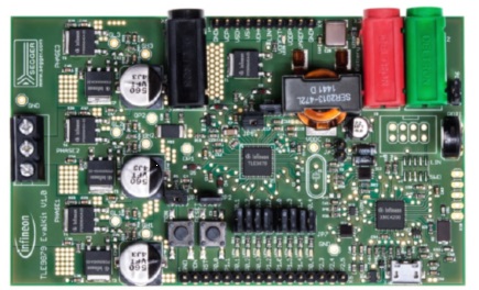
ͼ5.������TLE9879 EvalKit V1.3����ͼ
ͼ6.������TLE9879 EvalKit V1.3��ͼ
ͼ7.������TLE9879 EvalKit V1.3�ڲ�����ͼ
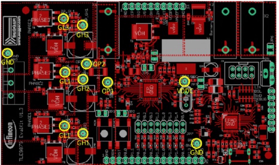
ͼ8.������TLE9879 EvalKit V1.3���Ե�ͼ
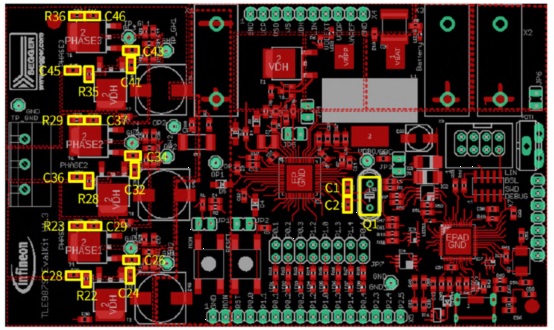
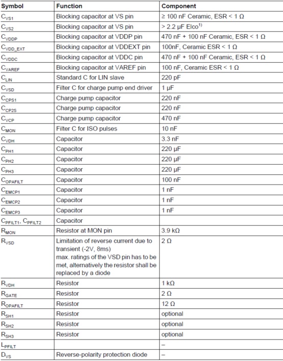
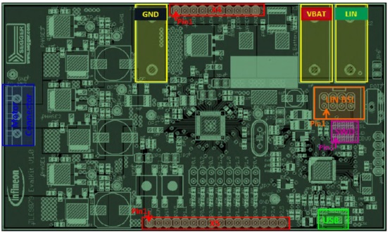
ͼ9.������TLE9879 EvalKit V1.3����Ԫ�����õ�ͼ
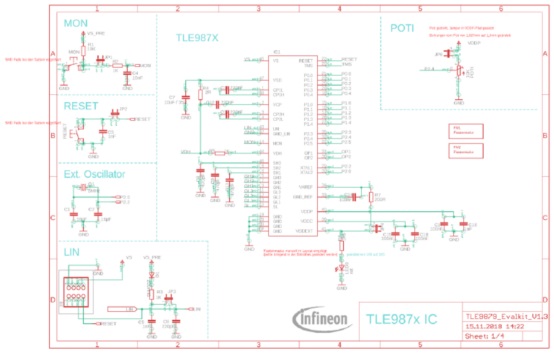
ͼ10.������TLE9879 EvalKit V1.3��·ͼ(1)
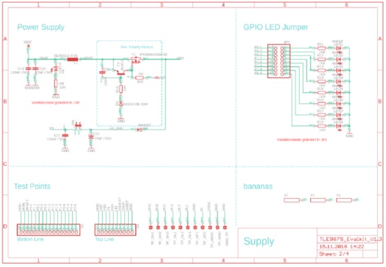
ͼ11.������TLE9879 EvalKit V1.3��·ͼ(2)
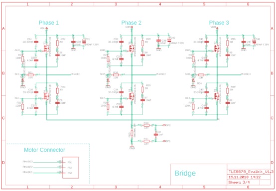
ͼ12.������TLE9879 EvalKit V1.3��·ͼ(3)
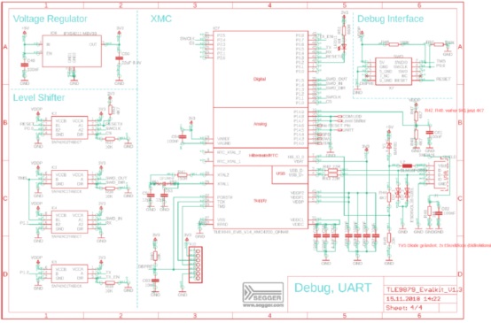
ͼ13.������TLE9879 EvalKit V1.3��·ͼ(4)
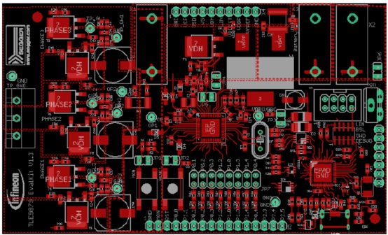
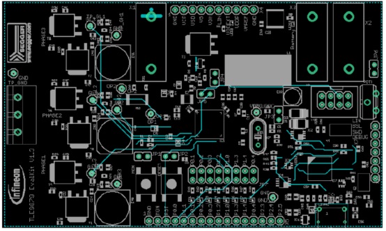
ͼ14.������TLE9879 EvalKit V1.3 PCB���ͼ(1):����
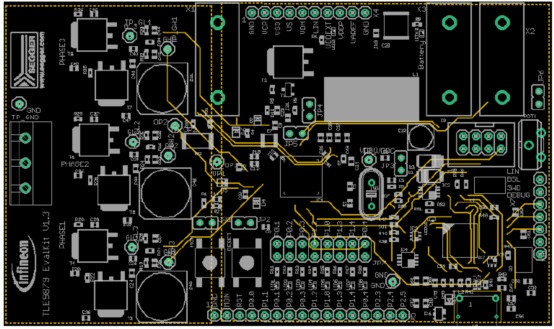
ͼ15.������TLE9879 EvalKit V1.3 PCB���ͼ(1):��2
ͼ16.������TLE9879 EvalKit V1.3 PCB���ͼ(1):��3
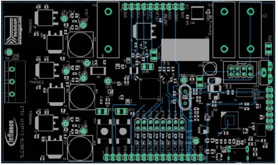
ͼ17.������TLE9879 EvalKit V1.3 PCB���ͼ(1):�ײ�
|
|
| |
| |
|
|
|