 |
|
| |
|
|
业务洽谈:
联系人:张顺平
手机:17727550196(微信同号)
QQ:3003262363
EMAIL:zsp2018@szczkjgs.com
联系人:鄢先辉
手机:17727552449 (微信同号)
QQ:2850985542
EMAIL:yanxianhui@szczkjgs.com
负责人联络方式:
手机:13713728695(微信同号)
QQ:3003207580
EMAIL:panbo@szczkjgs.com
联系人:潘波 |
|
|
| |
|
 |
|
 |
当前位置:首页 -> 技术分享 |
|
|
| SSM3582 2x31.76W数字输入无滤波器D类放大器解决方案 |
|
|
| 文章来源:永阜康科技 更新时间:2019/12/25 10:24:00 |
|
ADI公司的SSM3582是2x31.76 W高效数字输入无滤波器立体声D类放大器,可以工作在单电源,仅需要很少的外接元件,从而大大降低了电路的材料清单.器件采用扩频Σ-Δ调制,能直接和扬声器连接,和其它D类架构相比,保证了最好的模拟性能而同时降低了电磁辐射,可选择超低电磁干扰(EMI)模式,大大降低了100MHz以上的辐射,从而可以使用更长的扬声器电缆.放大器具有杰出的模拟性能,信噪比为106dB,总失真+噪音(THD+N)为0.004%. SSM3582A工作电压为单电源4.5 V 到16 V ,能向8 Ω 和4 Ω负载以小于1% THD提供2x15W rms连续功率.功率效率8 Ω负载为93.8%,4 Ω负载为90.6%.脉码调制(PCM)音频串口支持大多数协议如I2S,左侧调整, 时分复接(TDM),以及单个接口上寻址多达16个器件,多达32个音频播放通路.器件具有短路保护,欠压保护和热保护.主要用在移动计算,全合一计算机,手持电子学,无线扬声器和电视机.本文介绍了SSM3582主要特性,功能框图和立体声和单声道放大器应用电路,以及评估板EVAL-SSM3582Z主要特性,框图,电路图,材料清单和PCB设计图.
The SSM3582A is a fully integrated, high efficiency, digital input stereo Class-D audio amplifier. The device can operate from a single supply and requires only a few external components, significantly reducing the circuit bill of materials.
A proprietary, spread spectrum Σ-Δ modulation scheme enables direct connection to the speaker and ensures state-of-the-art analog performance while lowering radiated emissions compared to other Class-D architectures. An optional ultralow electromagnetic interference (EMI) mode significantly reduces radiated emissions above 100 MHz, enabling longer speaker cable lengths. Audio is transmitted digitally to the amplifier, minimizing the possibility of signal corruption in digital environments. The amplifier provides outstanding analog performance, with a 106 dB signal-to-noise ratio and a low 0.004% total harmonic distortion + noise (THD + N).
The SSM3582A operates from a single 4.5 V to 16 V supply and is capable of delivering 2× 15 W rms continuously into 8 Ω and 4 Ω loads at <1% total harmonic distortion (THD). The efficient modulation scheme maintains excellent power efficiency over a wide range of impedances: 93.8% into an 8 Ω load and 90.6% into a 4 Ω load. Optimization of the output pulse maintains performance at impedances as low as 3 Ω/5 μH, enabling its use with extended bandwidth tweeters.
The pulse code modulation (PCM) audio serial port supports most common protocols, such as I2S, left justified, and time division multiplexing (TDM), and can address up to 16 devices on a single interface, for up to 32 audio playback channels.
IC operation is controlled through a dedicated I2C interface. The two ADDRx pins (2×, five-level) define up to 16 individual addresses in I2C and standalone modes and automatically set the default TDM slots attribution.
A micropower shutdown mode is triggered by removing the digital audio interface clock, with a typical current of <1 μA. A software power-down mode is also available.
An automatic power-down feature shuts down the amplifier and the digital-to-analog converter (DAC) when no signal is present at the input, minimizing power consumption during digital silence. The device restarts when nonzero data is present at the input. Mute and unmute transitions are pop and click free.
The SSM3582A is specified over the commercial temperature range of −40℃to +85℃. The device has built in thermal shutdown and output short-circuit protection, as well as an early thermal warning with programmable gain limiting to maintain operation.
The SSM3582A is available in a 40-lead, 6 mm × 6 mm lead frame chip scale package (LFCSP), with a thermal pad to improve heat dissipation.
SSM3582主要特性:
Digital input stereo, high efficiency Class-D amplifier
Operates from a single 4.5 V to 16 V supply
State-of-the-art, proprietary, filterless Σ-Δ modulation
106.5 dB SNR at PO = 8.1 W, RL = 8 Ω, AV = 19 dB, PVDD = 12 V, A weighted
0.004% THD + N at 5 W into 8 Ω
38.5 μVrms output voltage noise, f = 20 Hz to 20 kHz, A weighted, PVDD = 16 V, 8 Ω
Pop and clickless on and off sequence
2× 14.67 W output at 12 V supply to 4 Ω loads at <1% THD + N
2× 14.4 W output at 16 V supply to 8 Ω loads at <1% THD + N
Mono mode for increased maximum output power
1× 49.69 W output at 16 V supply to 2 Ω loads at <1% THD + N
Support for low impedance loads
As low as 3 Ω/5 μH in stereo mode
As low as 2 Ω/5 μH in mono mode
High power efficiency
93.8% efficiency into an 8 Ω load
90.6% efficiency into a 4 Ω load
12.34 mA quiescent current with single 12 V PVDD supply
Single-supply operation with internal LDOs or option to use an external 5 V and 1.8 V supply for lowest power consumption
I2C control and hardware modes with up to 16 pin-selectable slots/addresses
Supported sample rates from 8 kHz to 192 kHz with 24-bit resolution
Multiple PCM audio serial data formats
TDM slave with support for up to 16 devices on a single bus
I2S or left justified slave
Adjustable full-scale output tailored for many PVDD sources
2- and 3-cell Li-Ion batteries
Digital volume control with selectable smooth ramp
Automatic power-down function
Supply monitoring automatic gain control (AGC) function reduces system brownout
Standalone operational mode without I2C
Temperature sensor with 1°C step readout via I2C
Short-circuit, undervoltage, and thermal protection
Thermal early warning
Power-on reset
PVDD sensing ADC
40-lead, 6 mm × 6 mm LFCSP with thermal pad
SSM3582应用:
Mobile computing
All in one computers
Portable electronics
Wireless speakers
Televisions
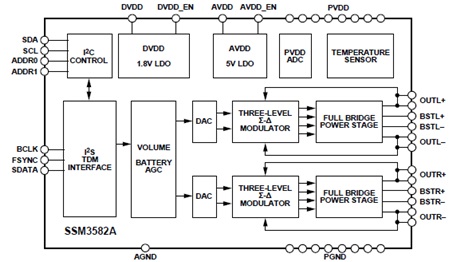
图1.SSM3582功能框图
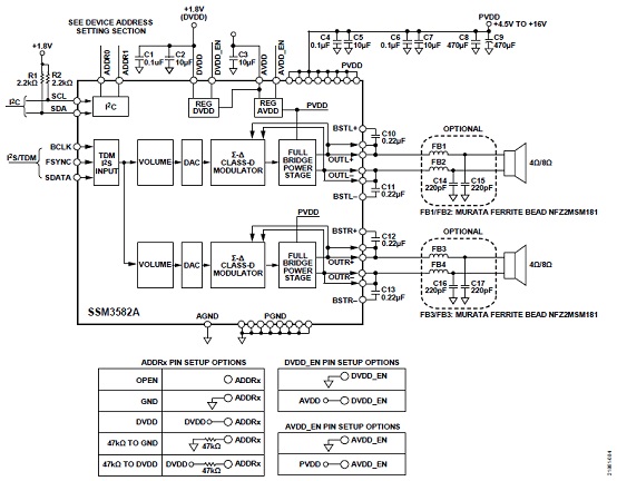
图2.SSM3582立体声输出应用电路图
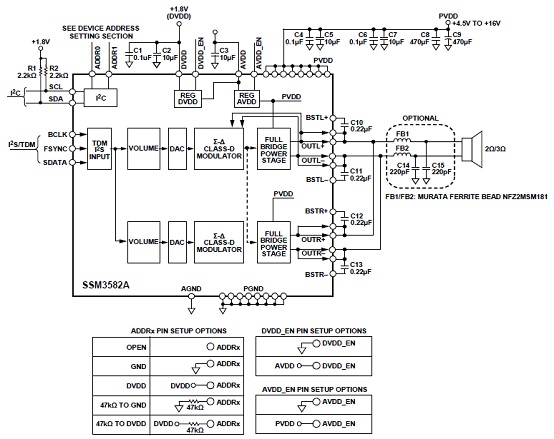
图3.SSM3582单声道输出应用电路图
评估板EVAL-SSM3582Z
Evaluating the SSM3582 or the SSM3582A 2×, 31.76 W, Digital Input, Filterless Stereo ClassD Audio Amplifier
The EVAL-SSM3582Z is the evaluation board for the SSM3582 or the SSM3582A, integrated stereo, 31.76 W, high efficiency, Class D, audio amplifiers with a digital input. This evaluation board can be used for both the SSM3582 or the SSM3582A devices.
The application circuit requires few external components and can operate from a single 4.5 V to 16 V supply. The EVAL-SSM3582Z is capable of delivering 14.67 W of continuous output power to a 4 Ω load from a 12 V power supply, with <1% THD + N, or 31.76 W into a 4 Ω load from 16 V, 10% THD + N.
The SSM3582 and the SSM3582A feature a high efficiency, low noise modulation scheme that requires no external reconstruction filter (LC) output filters. This scheme provides high efficiency, even at low output power.
The EVAL-SSM3582Z and the SSM3582 or the SSM3582A operate with 93.8% efficiency at 10 W into an 8 Ω load or 90.6% efficiency at 18 W into 4 Ω load from a 12 V supply. The EVAL-SSM3582Z, the SSM3582, and the SSM3582A have a typical noise floor of 38.5 μVrmsA weighted.
This user guide describes how to configure and use the EVAL-SSM3582Z. Read this user guide in conjunction with the SSM3582 and the SSM3582A data sheets, which provide specifications, internal block diagrams, a register map, and application guidance for the amplifiers.
评估板EVAL-SSM3582Z主要特性:
2×, 31.76 W into 4 Ω at16 V, THD + N = 10%
EVALUATION KIT CONTENTS
USBi USB interface board
USB cable
EVAL-SSM3582Z evaluation board
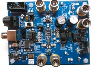
图4.评估板EVAL-SSM3582Z外形图(正面)
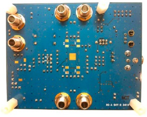
图5.评估板EVAL-SSM3582Z外形图(背面)
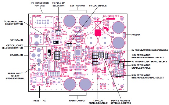
图6.评估板EVAL-SSM3582Z设定图
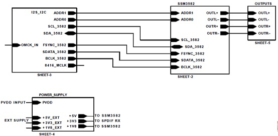
图7.评估板EVAL-SSM3582Z框图电路
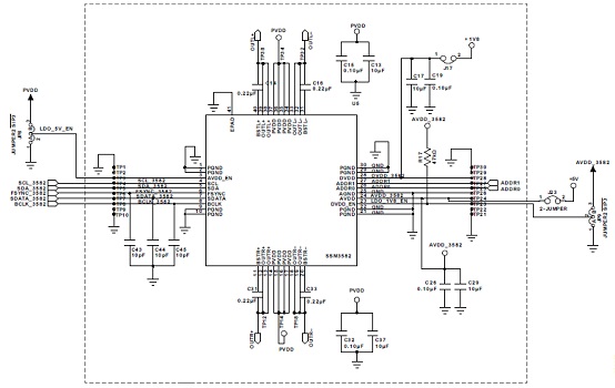
图8.评估板EVAL-SSM3582Z电路图:SSM3582部分
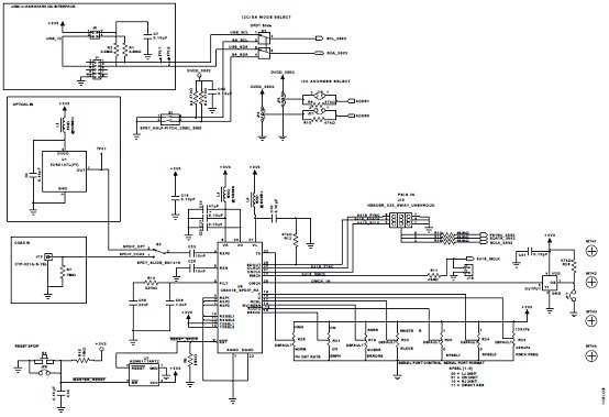
图9.评估板EVAL-SSM3582Z电路图:数字输入部分
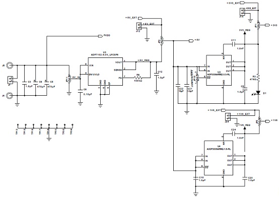
图10.评估板EVAL-SSM3582Z电路图:电源部分
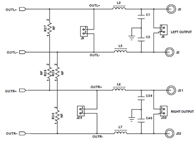
图11.评估板EVAL-SSM3582Z电路图:输出部分
评估板EVAL-SSM3582Z材料清单:
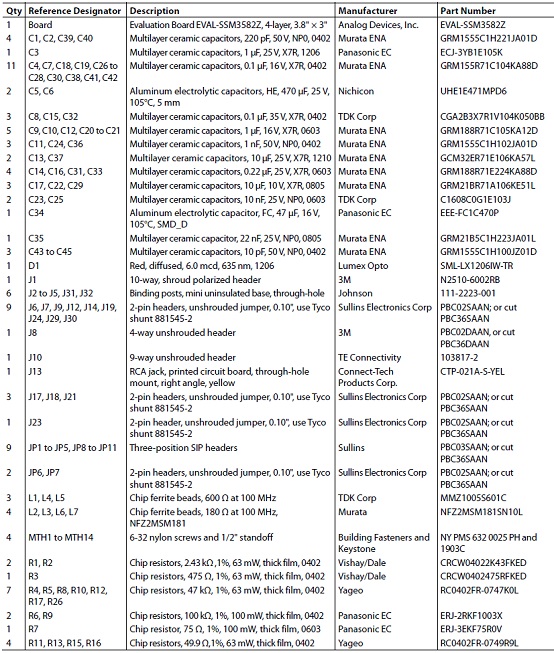
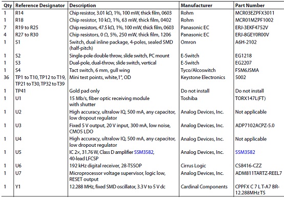
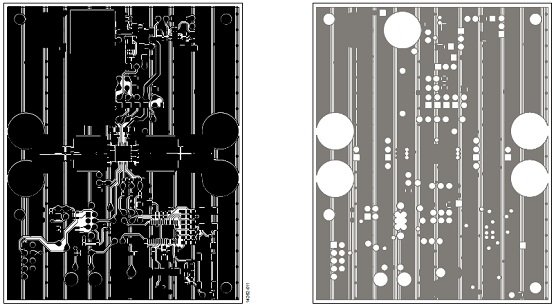
图12.评估板EVAL-SSM3582Z PCB设计图:左: 顶层,铜;右:第二层,铜
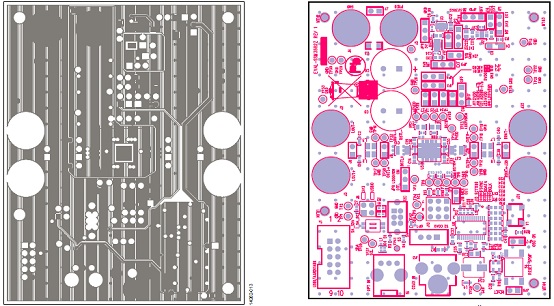
图13.评估板EVAL-SSM3582Z PCB设计图:左:第三层,铜;右:顶层,丝印
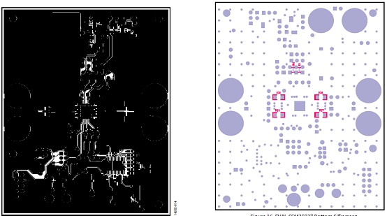
图14.评估板EVAL-SSM3582Z PCB设计图:左: 底层,铜;右:底层,丝印
|
|
| |
| |
|
|
|